33-99No. Mufu E Rd. Gulou District, Nanjing, China [email protected] | [email protected]
33-99No. Mufu E Rd. Gulou District, Nanjing, China [email protected] | [email protected]

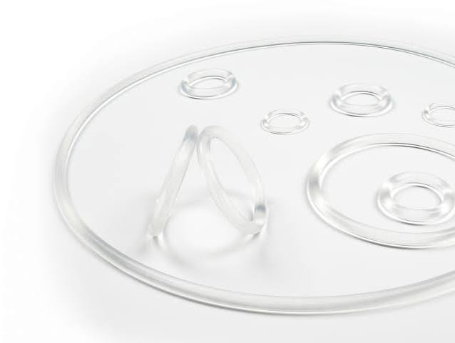
O-rings in semiconductor equipment are not "ordinary sealing parts," but the superposition of process contamination control, vacuum maintenance, chemical compatible parts, plasma consumables and traceable quality. Ordinary industrial scenarios mainly care about not leaking, corrosion resistance, aging resistance and long life; semiconductor scenarios must simultaneously prove they do not contaminate the wafer, chamber, gas path, ultra-clean system release organic matter, metal ions, ionic contaminants, particulate matter and other plasma corrosion byproducts, and this is the root cause of high O-ring requirements.
SIA's explanation of semiconductor pollution control can summarize this logic: device feature dimensions shrink and 3D structures grow more complex, making particles, impurities or other micro-contaminants likely to cause reliability or yield issues; semiconductor devices are also clearly sensitive to particulate, metal ions, chemistry, bacteria and space ion damage etc, highly sensitive. SEMI F51 also specially locks O-rings and sealing rings for outgassing discussion, the reason is that traditional ASTM or general industrial standards do not sufficiently comprehensively cover semiconductor sealing part performance evaluation, cleaning, packaging and other requirements.
O-rings in semiconductor equipment usually appear at chamber doors, chamber covers, observation windows, slit valve, vacuum flange, gas inlet/exhaust port, pump systems, wet bench, CVD/ALD/PECVD, etch, ash/strip and similar positions. It could directly touch process gas, plasma, strong acid-alkali, solvent, ultra-pure water, may also be subject to high temperature, vacuum, compression deformation, friction wear and periodic disassembly.
This leads its failure not simply "leaking or breaking." More typical failure paths are:
Sealing surface produces trace release, volatilization, dissolution, powder or particulate ion contamination → forms contamination on wafer surface or thin film → forms particulate defects, electrical anomalies, valve leakage, film adhesion abnormalities, corrosion/deposition uneven → yield decline or reliability risk.
SEMI F51's official abstract emphasizes it targets standards for semiconductor manufacturing equipment's sealing parts, and provides sealing material selection, performance judgment, cleanliness, packaging and processing information, to lower ownership cost and improve equipment uptime. This shows semiconductor O-ring's evaluation boundary has already "expanded" from rubber part to equipment usable rate, process stability and pollution control.
Semiconductor equipment's low outgassing risk includes three categories: one is real vacuum/high-temperature outgassing, that is elastomer's low-molecular volatile matter, residual monomer, crosslinking byproduct, additive, adsorbed moisture released into gas; two is liquid media leachables/extractables, that is metal ions, anions, TOC extracted from UPW, acid-alkali or solvent; three is process action decomposition products, e.g. plasma, strong oxidizer or ammonia/oxygen-containing gas cause sealing material surface degradation to produce migration contaminants.
Vacuum systems commonly reference ASTM E595 for this outgassing testing framework. NASA's explanation of ASTM E595 is, this method is used for measuring mass loss and re-condensable volatile matter of materials in vacuum, NASA data mentions early low-outgassing screening guideline TML ≤ 1.0% and CVCM ≤ 0.10% such judgment; but this testing idea explains why vacuum environment needs to focus on 'recondensable material,' not just leak rate.
In wet method, UPW transport scenarios, SEMI F57 is more directly relevant, CT Associates' explanation of SEMI F57 shows, this specification is applicable to high-purity polymer materials and parts, focusing on UPW inline immersion metal, anions and organic contamination; sample per SEMI F40 at 85°C UPW extraction 7 days. This type of testing logic is equally important for O-ring, because sealing parts are not passive spectators, but potential contamination sources in long-term soaking, compression, thermal cycling and media flushing.
Metal ion contamination is one of the easiest to underestimate problems in semiconductor sealing parts. O-ring's metal source is diverse: filler, pigment, additive system, processing aid, mold flash, grinding/repair residue, cleaning water, packaging material, human contact and environment settling, ordinary industrial rubber's acceptable ash, filler or metal residue, in the semiconductor front-end process could all become unacceptable electrical contamination sources.
ScienceDirect's article on "Essential high-purity sealing materials for semiconductor manufacturing" points out, metal ions can penetrate polymers, interface and expand toward diffusion, and metal contamination can lead to killer defects; the article also indicates, semiconductor sealing material selection needs to strictly control against high-purity sealing conditions through configuration, extrusion, molding, cleaning and packaging and production. UCT ChemTrace's SEMI F51-1115 series data also treats leachables, bulk trace metals, outgassing, TOC as monitoring objects for O-rings and sealing rings, and lists the leachable and bulk trace metal data differences of the same supplier's O-ring.
The key point is here: "same material name" does not equal "same metal ion level." Even called the same FFKM, FKM or EPDM, different formulation, different filler, different crosslinking system, different post-processing and different batch's metal background may be entirely different. What semiconductor customers truly purchase is "low metal ion contamination's configuration system + clean manufacturing + batch data," not material family name.
Key metal/ion categories to focus on control include:
Category |
Typical Elements |
Main Risk |
Alkali metal/movable ion |
Na, K, Li |
MOS/dielectric layer electric shift, threshold change, reliability risk |
Alkaline earth metal |
Ca, Mg, Ba, Sr |
Surface contamination, membrane anomaly, particulate/residue risk |
Transition metal |
Fe, Ni, Cr, Cu, Zn, Mn |
Leakage current, complexation, thin film and gate oxide reliability issue |
Process sensitive elements |
Al, Ti, Zr etc |
Thin film contamination, etch/deposition abnormal, wafer memory effect |
Semiconductor O-ring's particulate risk has four sources: first, molding, forming, repair, secondary processing left burrs, cracks, micro-debris; second, transportation and installation process friction, pulling, twisting and contamination cause new particulates; third, on and off position such as gate valve, slit valve, pump, flange positions dynamic wear generated; fourth, plasma or chemical media corrosion, material surface powdering, coarsening or carbonization etc.
ISO 14644-1:2015 explains, cleanroom air cleanliness particle-density is classified, particle size range covers 0.1 μm to 5 μm; semiconductor scenarios not only care about clean space air particle, still need concern surface particle, liquid-phase particle, gas transport system particle contribution; SEMI SCIS material, SEMI F114 and F115 are respectively applied to measuring particle and total re-precipitated particle count of UHP chemical delivery systems and wet processing partial equipment surfaces, this shows semiconductor industry has treated "parts self-contribute particulate/organic matter" as system-level metric.
For O-rings, low particulate is not something 'cleaned once and done.' Must start from formulation, use less or cautiously use loose filler; optimize mold, reduce burr and post-processing damage; use less contact cleaning; cleanroom packaging; and verify friction particulate and ion release after installation.
Parker's semiconductor installation guide splits elastomer concerns by plasma/gas deposition, thermal and wet three types of processes, where plasma/gas deposition concerns etch rate, particle generation, particle size, wet process concerns chemical compatibility and metal ion extractables. This exactly indicates semiconductor O-ring's particulate control must be positioned by process, not use one generic cleanliness grade rating.
The plasma inside semiconductor dry-process technologies is not just "gas," it includes ions, free radicals, UV, thermal load and physical bombardment, and its damage mechanism differs from liquid chemical corrosion. Oxygen and other ion volumes can oxidize/corrode rubber skeleton, fluorine-containing ion may cause surface changes, material "corrosion resistant" against liquid chemicals does not represent it being resistant to low outgassing, low particulate under plasma.
PPE's plasma processes material explicitly points out plasma sealing's chemical and thermal challenges are severe, key position's sealing material eventually all decays over time, and there is no single sealing material applicable to all chemical systems, tool position and product type; Parker's semiconductor sealing guide also commonly lists plasma/gas deposition chemistry including F, Cl, ClF₃, O₂, CF₄, O₃, SiH₄, C₂F₆, NF₃, WF₆ etc, and lists etch rate, particle generation, particle size as typical focus points.
Therefore, the key of using FFKM for semiconductor is not "FFKM being expensive," but that certain high-purity FFKM formulations provide better balance in strong corrosion, containing fluorine, vacuum, high temperature and low contamination requirements. Trelleborg's semiconductor characteristics describes advanced FFKM as high stability, high purity, super low trace metal, and emphasizes its lowering high-purity environment plasma resistance, but this does not mean 'all FFKM' are naturally qualified, filler, crosslinking system, post-processing, cleaning manufacturing and batch control, are equally important as material family name.
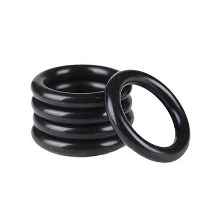
Many enterprises only value material selection, ignore packaging, storage, transport, opening, temporary storage, tool and manual assembly and other links. If the packaging material itself precipitates organic matter, fibers, or unclean sealing installation process is contaminated by hand contact, environment settling or improper cleaning packaging opening front lead time exposed, all seal treatments could be wasted.
SEMI F51's official abstract explicitly includes seal cleanliness, packaging and handling information, purpose being maintaining sealing part's best performance. ISO 14644-1's air cleanliness classification is applicable to independently defining packaging materials, packaging environment and double-layer packaging themselves, not clean packaging's independence.
High-end semiconductor O-rings usually should treat clean packaging as a specification field, not a physical attribute. It is recommended to write in the white paper this way:
Product goes through clean cleaning, clean environment inspection and clean packaging then delivery; internal and external bag material meets low particulate, low metal ion, organic volatile requirement; each packaging unit has batch number, material, specification, cleaning batch, inspection status and traceability identification.
Ordinary O-ring's batch consistency usually focuses on dimension, hardness, tensile, compression permanent deformation. Semiconductor O-rings must also focus on contamination data consistency, e.g. metal ion, TOC, anion, particulate, outgassing and other batch data's uniformity.
UCT ChemTrace's data shows, O-ring may reference SEMI F51-1115 for leachables, trace metals, bulk trace metals, outgassing, TOC etc for qualification and monitoring, and end user will use these data compared to supplier, appointed dedicated process application. This means semiconductor O-ring supplier cannot only claim 'this batch passed,' but must be able to prove 'batch fluctuation is controllable.'
Core control points of batch consistency include:
Link |
Control Content |
Raw Material |
Polymer batch, filler batch, crosslink agent batch, processing aid batch, metal background |
Compound Mixing |
Compounding equipment cleanliness, cross-contamination, formulation version, batch number |
Molding |
Mold material condition, demolding method, curing curve, sealing traceability |
Post-Processing |
Post-cure, cleaning, baking, dry, outgassing |
Inspection |
Dimension, particle, ion, metal, organic matter, outgassing |
Packaging |
Packaging material batch, clean environment, double bag, label, outgassing transfer |
Change |
Formulation, raw material, mold, cleaning agent, packaging material change notification |
One reason semiconductor customer's traceability requirement is high, is because contamination anomaly is often not exposed at installation moment. One sealed part batch could affect a certain equipment, a certain chamber, a certain PM cycle or a certain batch wafer or similar batch-type parameters. If cannot trace back to wafer anomaly from equipment location, sealing batch, material batch and cleaning number or the like, fault analysis cost will greatly rise.
SEMI SCIS data shows, industry standardization work includes traceable verification, part exchange, data exchange and other directions. This means traceability already not single-company quality bias, but part of semiconductor industry's uniform standardization trend.
High-end semiconductor O-ring traceability at least should include:
File/Data |
Function |
COC/COA |
Prove material, specification, batch and inspection status |
Material Batch Number |
Trace back polymer, filler, crosslinking system configuration version |
Production Batch Number |
Trace back mixing, molding, post-cure, cleaning and packaging |
Cleanliness Inspection Report |
Particle, metal ion, anion, TOC, outgassing |
Dimension/Appearance Report |
Ensure assembly reliability and surface defects |
Packaging Record |
Prove clean package state and material particulate |
Change Record |
Support PCN, customer approval and anomaly investigation |
Installation Location Record |
Connect equipment, chamber, PM cycle and wafer lot |
FFKM's advantage is full fluorine or highly fluorinated structure bringing better chemical stability, thermal stability and low reactivity. SIA's PFAS/fluorine-containing material background documents mention, semiconductor equipment and related materials need inertness, purity, wide chemical and thermal stability, low friction, electrical properties and other combined characteristics. In plasma, CVD, etch, ALD, wet chemistry and vacuum applications, these characteristics indeed make high-purity FFKM become the important selection at key sealing positions.
But must avoid three misconceptions:
First, material family name is not equal to cleanliness grade. FFKM can be semiconductor grade, also can be ordinary industrial grade; difference comes from formulation, filler, crosslinking system, purification, post-processing, cleaning, packaging and inspection.
Second, chemical resistance is not equal to low pollution. A material could resist HF, HCl, O₂ plasma or NF₃, but still could have relatively high metal extraction, relatively high particulate release or relatively high organic volatilization. Parker's material list can indeed be seen the same semiconductor material family distinguishes low particle generation, low extractables, metal extractables, etch rate etc different attributes.
Third, low erosion rate is not necessarily low particulate. Certain filled materials may have lower ion erosion rate, but filler or surface degradation layer may bring particles; certain non-filled materials particles may be less, but in certain plasma the life may not be longest. Therefore key position must select per process gas system, power, temperature, pressure, distance from ion source and PM cycle.
Application Position |
Main Media/Environment |
Most Related Requirement |
Recommended Focus Indicator |
Etch chamber |
O₂, CF₄, C₄F₈, SF₆, Cl₂, HBr, BCl₃ and other plasma |
NF₃ ion resistance high, particle release, low metal, etch rate |
Low plasma erosion, particle release, metal extractables, compression permanent deformation |
Ash/strip |
O₂, CF₄, NH₃, N₂O, TE etc oxidizing plasma |
High-temperature stability, O₂ plasma resistance, low particle, low outgassing |
Surface change, particle, outgassing |
PECVD/ALD/CVD |
SiH₄, NH₃, N₂O, NF₃, O₂, etc |
High-temperature stability, low outgassing, low metal ions |
TML/CVCM, GC-MS, metal ions, compression set |
Wet chemical delivery |
HF, HCl, H₂SO₄, SC1, SC2, KOH, NaOH, UPW etc |
Low dissolution, chemical resistance, SEMI F57 class extraction, TOC, low anion |
Low dissolution, TOC, metal ions |
Lithography/track |
Solvent, developer, photoresist related chemicals |
Low organic release, low swelling |
Organic outgassing, low swelling |
Slit valve/door seal |
Low vacuum, sliding friction, weekly compression |
Low abrasive particulate, dimension stability, surface integrity |
Particle generation, size stability, surface defects |
Vacuum pump/exhaust |
Corrosive byproducts, heat, vacuum, chemical backflow contamination |
Corrosion resistance, life, outgassing, corrosion after backflow contamination |
Outgassing, PM cycle |
Gas delivery seal |
UHP gas, pressure follow |
Low particle, low metal, low permeation, dense seal |
Particle contribution, leak rate, metal/organic contamination |
It is recommended to upgrade semiconductor O-ring specification from "material specification sheet" to "pollution control specification sheet." Can establish by the following fields:
Module |
Recommended Field |
Basic Information |
Material family; specific compound; hardness; color; dimension standard; drawing number |
Process Position |
chamber, valve, gas line, wet, UPW, vacuum, pump, lithography |
Process Conditions |
Temperature, pressure/vacuum, media, plasma type, RF power, exposure time, PM cycle |
Precipitates/Volatilization |
TML, CVCM, GC-MS, TOC, extractable organic matter, baking conditions |
Metal Ions |
ICP-MS/VPD-ICP-MS; Na, K, Li, Fe, Ni, Cr, Cu, Al, Ca, Mg, Zn etc |
Anions |
F⁻, Cl⁻, NO₃⁻, SO₄²⁻, PO₄³⁻ etc |
Particles |
Surface particles, liquid phase extraction particles, dynamic friction particles, plasma post-particles |
Mechanical Properties |
Compression permanent deformation, tensile, elongation rate, hardness, thermal expansion coefficient, dimension tolerance |
Cleaning Process |
Cleanroom grade, cleaning flow, drying, inspection, personnel/environment control |
Clean Packaging |
Double bag, packaging material, label, unpacking requirements, retention period |
Batch Consistency |
Raw material batch number, formulation version, production batch, trend data |
Traceability |
COC/COA, inspection report, PCN, anomaly investigation, customer approval record |
Semiconductor equipment's high requirement for O-rings is not because customer wants to "pay for expensive material," but because O-rings are at the intersection of vacuum, plasma, strong corrosive chemicals, cleanroom, nano-level structure and high yield production. Its value is not in "being able to seal," but instead in:
Sealing reliable + low precipitates + not outgassing + not shedding particles + not releasing metal ions + resisting plasma + clean packaging + batch consistent + traceable.
Therefore, semiconductor O-rings should be positioned as high-end process consumables and pollution control parts. The core viewpoint of the white paper can be written as:
In semiconductor equipment, O-ring's competitiveness is not material unit price, but the comprehensive result of pollution budget, process uptime, PM cycle, yield risk and supply chain traceability capability. FFKM is only the entry ticket; high purity, low precipitates, low particulate, low metal ion, ion resistance and clean delivery system, are the truly deciding barrier.

Welcome to HOVOO, a Chinese seal factory. Production of PU, Rubber and PTFE seals. The seals include O-ring, piston seal, rod seal, Gray ring and gas seal.


 EN
EN
 AR
AR CS
CS DA
DA NL
NL FI
FI FR
FR DE
DE EL
EL IT
IT JA
JA KO
KO NO
NO PL
PL PT
PT RO
RO RU
RU ES
ES SV
SV TL
TL IW
IW ID
ID LV
LV SR
SR SK
SK VI
VI HU
HU MT
MT TH
TH TR
TR FA
FA MS
MS GA
GA CY
CY IS
IS KA
KA UR
UR LA
LA TA
TA MY
MY
